MESSAGE
Nagoya University)
“CRYSTAL DEFECT CORE” PROJECT HAS LAUNCHED!
Since occurrence of the human civilization, epoch-making innovations in fields of environmental conservation, energy development and information technology have been realized by emergence of novel and advanced materials of metals, ceramics, and semiconductors. In this regard, it is not too much to say that materials science has played an essential role for them in history of mankind. In the current complicated, diversified and globalized modern societies, however, timely development of unprecedented materials is indispensable and highly desired. Therefore, it is necessary to conduct materials development based on a new concept in materials science.
In this project, we firmly conduct fundamental and scientific researches on the structure property relationships in crystal defects of materials at the nanometer scale. This is because crystal defects such as grain boundaries, interfaces and dislocations are found to become physical origins of distinct properties in recent advanced materials. Moreover, scientific attempts are now being done in advanced-material development by designing and controlling physical properties of crystal defects at the nanometer scale. If we know how to maximize potentials of physical properties of crystal defects, such knowledge should provide us with breakthroughs in materials science. Then, it should be an indispensable step to systematically reveal nature of specific electronic and atomic structures at crystal defects, especially at their core regions.
Here we refer to specific electronic and atomic structures localized at crystal defects as “crystal defect cores”, and try to establish the new materials science. For this purpose, researchers specializing in theoretical calculations, nanoscale characterization and advanced materials processing conduct collaborative studies. Establishment of new scientific principles based on the concept of “crystal defect core” will make it possible to explore novel materials with excellent properties due to crystal defects.
RESEARCH
PURPOSE OF THE RESEARCH PROJECT
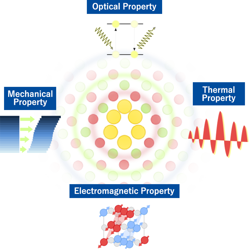
In this project, specific electronic and atomic structures of grain boundaries, interfaces and dislocations that can realize novel and distinct materials properties are defined and referred to as “crystal defect cores”. Researchers specializing in theoretical calculations, nanoscale characterization and advanced materials processing conduct collaborative studies, aiming at creating a new area in materials science named “crystal defect core”. Through establishing new scientific principles based on the concepts of “crystal defect core”, we will further explore novel properties and materials due to crystal defects.
Conventional studies have focused on average bulk structures and macroscopic properties of materials in general, and thus understanding of crystal defects is often limited to their static and averaged atomic pictures. Recent technological progresses in methods and approaches of nanoscale characterization and computational science are so remarkable that we have been enabled to acquire quantitative information on nanoscale structures of crystal defects. These advanced approaches and methods have facilitated our more in-depth understanding about the crucial roles that the crystal defects play for realizing various materials properties. For future materials design and development, it is essential to reveal relationships between nanoscale structures of crystal defects and materials properties. Thus, in this project, we aim at discovering or creating new materials functions and new exploratory materials based on “crystal defect cores”, including those emerging under external stimulus including thermal, electric, magnetic, optical or stress fields.
CONTENT OF THE RESEARCH PROJECT
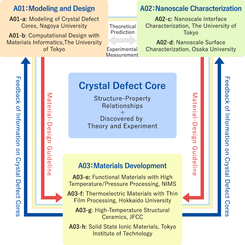
This research project has three major research items as follows:
- A01: Modeling and design of crystal defect cores
- A02: Nanoscale characterization of crystal defect cores
- A03: Materials development based on crystal defect cores
In research items A01 and A02, we focus on basic science of crystal defects. We do collaborative and systematic researches of grain boundaries, interfaces and dislocations so as to establish new scientific principles based on in-depth understanding of a structure-property relationship of the crystal defects, by means of theoretical calculations, materials informatics and nanoscale characterization at the world-class highest level. Researches in the Research item A03 of materials processing come from diverse materials fields, and try to develop novel materials and their properties by controlling crystal defects at the nanometer scale. Throughout the research area, it is expected for our intensive and extensive collaborations to prove that “crystal defect core” is a universal concept to realize novel materials development in the next generation.
EXPECTED RESEARCH ACHIEVEMENTS
- To establish new scientific principles to make it possible to explore novel and distinct materials properties originating from crystal defects
- To discover or create new materials with remarkable properties in diverse fields of materials science
- To facilitate considerable technical development of theoretical calculations, nanoscale characterization, and materials processing
EXPECTED SCIENTIFIC SIGNIFICANCE
Our concept of “crystal defect core” will provide a scientific impact when we succeed in developing materials and their properties through precisely controlling crystal defect cores. This is because crystal defects have been thought to play a negative role for materials properties. This research area can find out a new strategy for controlling crystal defect cores so that they play positive roles for better properties, paving a new avenue for future materials developments.
MEMBER
EXECUTIVE COMMITTEE
| Katsuyuki Matsunaga (Nagoya University) | Teruyasu Mizoguchi (The University of Tokyo) |
|---|---|
| Naoya Shibata (The University of Tokyo) | Masayuki Abe (Osaka University) |
| Hitoshi Yusa (National Institute for Materials Science) | Hiromichi Ohta (Hokkaido University) |
| Satoshi Kitaoka (Japan Fine Ceramics Center) | Masaaki Hirayama (Tokyo Institute of Technology) |
| Masato Yoshiya (Osaka University) | Atsutomo Nakamura (Osaka University) |
| Hidehiro Yoshida (The University of Tokyo) | |
EVALUATION COMMITTEE MEMBERS
| Taketo Sakuma (The University of Tokyo, Emeritus Professor) |
|---|
| Hirotarou Mori (Osaka University, Invited Professor) |
| Seizo Morita (Osaka University, Emeritus Professor) |
| Masanori Kohyama (National Institute of Advanced Industrial Science and Technology, Emeritus Researcher) |
RESEARCH AREA ADVISORS
| Isao Tanaka (Kyoto University, Professor) |
|---|
| Yuichi Ikuhara (The University of Tokyo, Professor) |
EXTERNAL EXAMINER
| Hikaru Kuramochi (Institute for Molecular Science, Associate Professor) |
|---|
| Yoshinobu Kawahara (Osaka University, Professor) |
RESEARCH ITEMS AND GROUPS
A01Modeling and Design of Crystal Defect Cores
A01-aModeling of Crystal Defect Cores
| Group Leader |
|
|---|---|
| Member |
A01-bComputational Design with Materials Informatics
| Group Leader |
|
|---|---|
| Member |


A02Nanoscale Characterization of Crystal Defect Cores
A02-cNanoscale Interface Characterization
| Group Leader |
|
|---|---|
| Member |
|

A02-dNanoscale Surface Characterization
| Group Leader |
|
|---|---|
| Member |
|
A03Materials Development Based on Crystal Defect Cores
A03-eFunctional Materials with High Temperature/Pressure Processing
| Group Leader |
|
|---|---|
| Member |
|
A03-fThermoelectric Materials with Thin Film Processing
| Group Leader |
|
|---|---|
| Member |
|

A03-gHigh-Temperature Structural Ceramics
| Group Leader |
|
|---|---|
| Member |
A03-hSolid State Ionic Materials
| Group Leader |
|
|---|---|
| Member |
ACHIEVEMENT
2023.12.29 Yuqiao Zhang* & Hiromichi Ohta*, “Recent progress in thermoelectric layered cobalt oxide thin films”, NPG Asia Mater. 15, 67 (2023). (December 29, 2023) (DOI: 10.1038/s41427-023-00520-w)
2023.12.15 S. Fujii, A. Kuwabara, Interatomic potentials for cubic zirconia and yttria-stabilized zirconia optimized by genetic algorithm, Comput. Mater. Sci., 233 (2024) 112722. (DOI: 10.1016/j.commatsci.2023.112722)
2023.11.01 S. Fujii, K. Shimazaki, A. Kuwabara, Empirical interatomic potentials for ZrO2 and YSZ polymorphs: Application to a tetragonal ZrO2 grain boundary, Acta Mater., 262 (2024) 119460. (DOI: 10.1016/j.actamat.2023.119460)
2023.10.20 Taishi Yokoi*, Masahiro Watanabe, Fumiya Nakamura, Hiromi Kimura-Suda, Masaya Shimabukuro and Masakazu Kawashita, “Formation of octacalcium phosphate with incorporated dicarboxylate ions containing disulfide bonds”, Dalton Transactions, 52, 16586-16590 (2023). (DOI: 10.1039/d3dt02462h) 【Back Cover】
2023.10.17 The 29th International Workshop on Oxide Electronics (iWOE-29) Best Presentation Award “Direct Thermal Conductivity Measurement for Freestanding Ba1/3CoO2 and Sr1/3CoO2 Films in the In-plane direction”
Kungwan Kang (Hokkaido University)2023.10.16 Kungwan Kang, Fumiaki Kato, Akitoshi Nakano, Ichiro Terasaki*, Takashi Endo, Yasutaka Matsuo, Hyoungjeen Jeen*, and Hiromichi Ohta*, “Fabrication and Thermoelectric Properties of Freestanding Ba1/3CoO2 Single-Crystalline Films”, ACS Appl. Electron. Mater. 5, 5749-5754 (2023). (DOI: 10.1021/acsaelm.3c01129)
2023.10.12 Karen Kuroyama, Ryuichi Fujikawa, Tomoyo Goto, Tohru Sekino, Fumiya Nakamura, Hiromi Kimura-Suda, Peng Chen, Hiroyasu Kanetaka, Tomoka Hasegawa, Kaname Yoshida, Masaru Murata, Hidemi Nakata, Masaya Shimabukuro, Masakazu Kawashita, Tetsuya Yoda, Taishi Yokoi*, “Development of damage-tolerant calcium phosphate bulk materials based on a bioinspired material design”, Science and Technology of Advanced Materials, 24, 2261836 (2023). (DOI: 10.1080/14686996.2023.2261836)
2023.10.03 Y. Li*, H. Oguri, A. Matsubara, E. Tochigi, X. Fang, Y. Ogura, K. Matsunaga, A. Nakamura, Strain-rate insensitive photoindentation pop-in behavior in ZnS single crystals at room temperature, Journal of the Ceramic Society of Japan, 131, 685-689 (2023). (DOI: https://doi.org/10.2109/jcersj2.23064)
2023.10.01 Taishi Yokoi*, Masahiro Watanabe, Yuejun Wang, Tomoyo Goto, Tohru Sekino, Masaya Shimabukuro, Masakazu Kawashita, “Synthesis and fluorescence properties of octacalcium phosphate with incorporated pyridinedicarboxylate ions”, Journal of the Ceramic Society of Japan, 131, 701-707 (2023). (DOI: 10.2109/jcersj2.23027)
2023.09.19 Rui Yu, Lizhikun Gong, Hiromichi Ohta, Tsukasa Katayama*, “Ferroelectricity, high permittivity, and tunability in millimeter-size crack-free Ba1–xSrxTiO3 flexible epitaxial sheets”, ACS Appl. Electron. Mater. 5, 5234-5239 (2023). (September 14, 2023) (DOI: 10.1021/acsaelm.3c00963)
2023.09.19 第54回(2023年春季)応用物理学会講演奨励賞 “Flexible BaTiO3 Epitaxial Films with Bulk-like Ferroelectricity and Piezoelectricity” Lithikun Gong (Hokkaido University)
2023.09.11 S. Fujii, Y. Shimizu, J. Hyodo, A. Kuwabara, Y. Yamazaki, “Discovery of Unconventional Proton-Conducting Inorganic Solids via Defect-Chemistry-Trained, Interpretable Machine Learning”, Adv. Energy Mater. 202301892 (2023). DOI: 10.1002/aenm.202301892
2023.07.29
Maya Matsuura, Tatsuya Yokoi*, Yu Ogura, Katsuyuki Matsunaga, Anharmonicity in grain boundary energy for Al: thermodynamic integration with artificial-neural-network potential, Scripta Materialia, 236 (2023) 115685.(DOI: https://doi.org/10.1016/j.scriptamat.2023.115685)2023.07.25
Mitsuki Yoshimura, Qian Yang, Zhiping Bian, and Hiromichi Ohta*, “Significant Reduction in the Switching Time of Solid-State Electrochemical Thermal Transistors”, ACS Appl. Electron. Mater. 5, 4233 (2023). (July 24, 2023) (DOI: 10.1021/acsaelm.3c00512)2023.06.20 The 4th Workshop on Functional Materials Science (FMS2023) Outstanding Presentation Award
“Carrier-trapping effects on glide dislocation cores in Cd compound semiconductors”
Sena Hoshino (Nagoya University)2023.06.20 The 4th Workshop on Functional Materials Science (FMS2023) Outstanding Presentation Award “Direct measurement of in-plane thermal conductivity for freestanding Ba1/3CoO2 films” Kungwan Kang (Hokkaido University)
2023.06.13
Bin Feng, Sena Hoshino, Bin Miao, Jiake Wei, Yu Ogura, Atsutomo Nakamura, Eita Tochigi, Katsuyuki Matsunaga, Yuichi Ikuhara and Naoya Shibata,
“Direct observation of intrinsic core structure of a partial dislocation in ZnS”,
Journal of the Ceramic Society of Japan, 131, 659-664 (2023). (DOI: https://doi.org/10.2109/jcersj2.23065)2023.05.08
Tatsuya Yokoi, Maya Matsuura, Yu Oshima, Katsuyuki Matsunaga, Grain-boundary thermodynamics with artificial-neural-network potential: Its ability to predict the atomic structures, energetics and lattice vibrational properties for Al, Physical Review Materials, 7 (2023) 053803. Published 17 May 2023.2023.05.08
Tatsuya Yokoi, Akihiro Hamajima, Yu Ogura, Katsuyuki Matsunaga, Grain boundary segregation of Y and Hf dopants in α-Al2O3: A Monte Carlo simulation with artificial-neural-network potential and DFT calculation, Journal of the Ceramic Society of Japan, 131, 751-761 (2023). (DOI: https://doi.org/10.2109/jcersj2.23044)2023.05.08
Sena Hoshino, Tatsuya Yokoi, Yu Ogura, Katsuyuki Matsunaga, Electronic and atomic structures of Shockley-partial dislocations in CdX (X = S, Se and Te), Journal of the Ceramic Society of Japan, 131, 613-620 (2023). (DOI: https://doi.org/10.2109/jcersj2.23055)2023.05.08
Yu Ogura, Yuki Tsuchiya, Sena Hoshino, Tatsuya Yokoi, Katsuyuki Matsunaga, Photoplastic effect in MgO single crystals, Journal of the Ceramic Society of Japan, 131, 628-631 (2023). (DOI: https://doi.org/10.2109/jcersj2.23060)2023.05.03
Zhiping Bian*, Qian Yang, Mitsuki Yoshimura, Hai Jun Cho, Joonhyuk Lee, Hyoungjeen Jeen, Takashi Endo, Yasutaka Matsuo, and Hiromichi Ohta*, “Solid-State Electrochemical Thermal Transistors with Strontium Cobaltite – Strontium Ferrite Solid Solutions as the Active Layers”, ACS Appl. Mater. Interfaces 15, 23512-23517 (2023). (May 3, 2023) (DOI:10.1021/acsami.3c03660)2023.04.17
Lizhikun Gong, Rui Yu, Hiromichi Ohta, and Tsukasa Katayama*, “Synthesis and transparent conductivity of crack-free La:BaSnO3 epitaxial flexible sheet”, Dalton Trans 52, 6317 (2023) (April 17, 2023) (DOI: 10.1039/d3dt01097j)2023.04.04
Binjie Chen, Chuchu Yang, Bin Feng, Yuichi Ikuhara, Hiromichi Ohta, Suppression of Strain Relaxation in VO2/TiO2 Multilayered Films, ACS Applied Electronic Materials 5, 2433-2438 (2023) (https://doi.org/10.1021/acsaelm.3c00246)2023.04.04
Y. Li*, X. Fang, E. Tochigi, Y. Oshima, S. Hoshino, T. Tanaka, H. Oguri, S. Ogata, Y. Ikuhara, K. Matsunaga, A. Nakamura, Shedding new light on the dislocation-mediated plasticity in wurtzite ZnO single crystals by photoindentation, Journal of Materials Science & Technology, 156, 206-216, 1 Sep. 2023 (DOI:https://doi.org/10.1016/j.jmst.2023.02.017)2023.04.01
Ryo Ishikawa, Shigeyuki Morishita, Toshiaki Tanigaki, Naoya Shibata, Yuichi Ikuhara, Spatial and phase resolution in electron microscopy, Microscopy, 72 (2) (2023) 78-96. (https://doi.org/10.1093/jmicro/dfac045)2023.03.23
Atsushi Tsurumaki-Fukuchi*, Takayoshi Katase, Hiromichi Ohta, Masashi Arita, and Yasuo Takahashi, “Direct Imaging of Ion Migration in Amorphous Oxide Electronic Synapses with Intrinsic Analog Switching Characteristics”, ACS Appl. Mater. Interfaces 15, 16842-16852 (2023). (March 23, 2023) (DOI: 10.1021/acsami.2c21568) OPEN ACCESS2023.03.20
Satoko Toyama, Takehito Seki, Yuya Kanitani, Yoshihiro Kudo, Shigetaka Tomiya, Yuichi Ikuhara, Naoya Shibata, Real-space observation of a two-dimensional electron gas at semiconductor heterointerfaces, Nature Nanotechnology, (2023) 1-8. (https://doi.org/10.1038/s41565-023-01349-8)2023.03.20
Z. Diao, K. Ueda, L. Hou, H. Yamashita, O. Custance, M. Abe, Automatic Drift Compensation for Nanoscale Imaging Using Feature Point Matching, Appl. Phys. Lett. 122 (12), (2023) 121601-1-6 (https://aip.scitation.org/doi/10.1063/5.0139330)2023.03.07
Y. Suzuki, Y. Imamura, D. Katsbe, A. Kogure, N. Hirai, M. Kimura, Visualization of Electrolyte Reaction Field Near the Negative Electrode of a Lead Acid Battery by Means of Amplitude/Frequency Modulation Atomic Force Microscopy, Materials 16(6), (2023) 21462023.03.03
F. Kawamura, Y. Shibazaki, H. Yusa, T. Taniguchi, High-pressure synthesis of Th3P4-type c-Zr3N4 Using a metathesis reaction and in situ X-ray diffraction studies of the formation process, Crystal Growth & Design. 23 [4] (2023) 2504-2510 (http://doi.org/10.1021/acs.cgd.2c01433)